IBM Debuts the World’s First Sub-1 Nanometer Chip — What the Angstrom Era Means for AI and for Investors
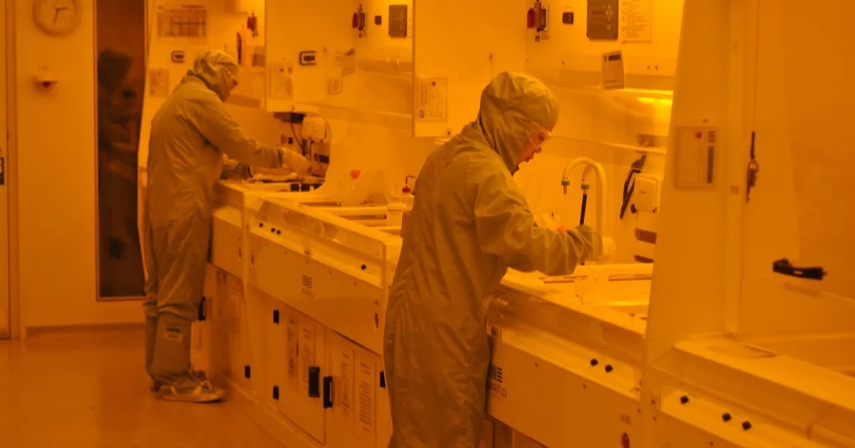
IBM has done it again. The company that produced the world’s first 2-nanometer chip back in 2021 says it has now demonstrated the first working transistors at a sub-1-nanometer node — the threshold the industry calls the “angstrom era,” where features are measured in tenths of a nanometer rather than whole ones. The breakthrough, unveiled from IBM’s Albany NanoTech Complex in upstate New York, is a research milestone rather than a product: a proof-of-concept test chip, not something you will find in a phone or a server this year. But it is a genuine marker on the long road of Moore’s Law, and it lands at precisely the moment the market is obsessed with the physical limits of artificial-intelligence compute.
The timing is not lost on anyone. This week the entire semiconductor complex melted up after Micron’s blowout earnings confirmed that the bottleneck in AI is shifting from raw logic to memory and packaging — and that demand for advanced silicon is structural, not cyclical. IBM’s announcement speaks to the other half of that story: how much further the logic itself can shrink, and who profits when it does. The short answer, as we will argue below, is that the most investable winners from a sub-1nm world are probably not IBM. They are the handful of companies that supply the tools and the manufacturing capacity to turn a lab demonstration into billions of chips.
Let’s unpack what IBM actually built, why “sub-1nm” matters, where the competitive race stands, and how an investor should think about the trade.
What IBM Actually Built
First, a reality check on the marketing. Process-node names like “2nm” or “sub-1nm” no longer describe any single physical dimension of a transistor — the actual gate lengths are larger than the label implies. They are generational shorthand for a new platform that is denser, faster, and more power-efficient than the one before it. With that caveat, here is what IBM’s disclosure represents.
From FinFET to nanosheet to CFET
For a decade, leading-edge chips used FinFET transistors. Around the 2nm generation, the industry switched to gate-all-around (GAA) nanosheet transistors, which wrap the gate fully around stacked horizontal channels for better control of current leakage. IBM pioneered exactly this design in 2021, packing roughly 50 billion transistors onto a fingernail-sized chip with three stacked silicon nanosheets. The path beyond 2nm runs through the complementary FET, or CFET — a structure that stacks an n-type and a p-type transistor directly on top of each other, roughly halving the footprint of a logic cell. IBM’s sub-1nm test chip uses a CFET-style stacked architecture as its foundation.
The 2D atomic channel
The harder problem at angstrom scale is the channel material itself. Silicon starts to misbehave when a channel is only a few atoms thick — electrons leak, and performance degrades. The frontier solution, long researched at IBM and the IMEC consortium, is to replace part of the silicon with two-dimensional materials: atom-thin sheets such as tungsten disulfide or molybdenum disulfide that conduct cleanly even at sub-nanometer thickness. Pairing a CFET structure with a 2D atomic channel is the conceptual leap that makes a credible sub-1nm transistor possible, and it is the part of IBM’s announcement that genuinely advances the science.
High-NA EUV and backside power
None of this can be patterned without the most expensive machine in the history of manufacturing: the High-NA extreme-ultraviolet (EUV) lithography system, built exclusively by the Dutch firm ASML at a list price north of $350–400 million per tool. IBM’s chip also relies on backside power delivery, which moves the power wiring beneath the transistors to free up routing space and cut resistance. These two enabling technologies — High-NA EUV for patterning and backside power for efficiency — are why the supplier ecosystem, not the announcing company, tends to capture the economics of each new node.
Why Sub-1nm Matters for AI
The reason this is a market story and not just an engineering footnote is power. Training and running large AI models is constrained less by the cost of chips than by the electricity and cooling they demand. Every shrink to a denser, lower-voltage node delivers more computation per watt — and at hyperscale, performance-per-watt is the whole game. A sub-1nm platform that offers materially better energy efficiency is, in effect, a lever on the operating cost of every AI data center built in the back half of this decade.
That ties IBM’s lab result directly to the supercycle the market has been pricing all week. Micron’s sold-out high-bandwidth memory, Nvidia’s accelerator backlog, and the global chip melt-up that sent the Nikkei to a record all rest on the same assumption: that the semiconductor roadmap will keep delivering more compute for the same power budget. A credible path below 1nm is a vote of confidence in that assumption — and a reminder that the roadmap, while slowing and growing fabulously expensive, has not hit a wall.
The Race to the Angstrom Era
IBM is a research powerhouse, but it does not manufacture leading-edge chips at scale. The companies that will actually ship angstrom-class silicon are the three remaining leading-edge foundries plus Japan’s IBM-backed newcomer, Rapidus. Here is roughly where the field stands.
| Player | Leading platform | Status | Role |
|---|---|---|---|
| IBM Research | Sub-1nm CFET + 2D channel | Lab test chip | Inventor / IP licensor |
| TSMC | N2 (2nm), A16, A14/A13 | 2nm in volume; A16 due H2 2026 | Leading-edge foundry |
| Intel | 18A (1.8nm), 14A next | 18A in high-volume manufacturing | Foundry + chipmaker |
| Samsung | SF2 (2nm), 1.4nm target | 2nm in production; 1.4nm ~2027 | Foundry + chipmaker |
| Rapidus | 2nm (IBM-licensed) | 2nm prototype line running | Japan foundry newcomer |
The key takeaway: a research demonstration at sub-1nm is years ahead of volume production. The industry is only now ramping 2nm into the market; commercial 1nm-class nodes are penciled in around 2027–2028, and true sub-1nm volume manufacturing is realistically a 2029–2031 story. IBM’s milestone shows the path is navigable — it does not shorten it.
IBM’s Real Business: Research, Not Fabs
This is the crux of the investment case, and where a lot of headline-driven enthusiasm goes wrong. IBM exited the business of manufacturing chips a decade ago. What it kept is one of the most productive semiconductor research operations on earth, anchored at its Albany NanoTech Complex, and it monetizes that research the way it monetizes most things now: through intellectual property, partnerships, and services. IBM has licensed its nanosheet and packaging technology to Rapidus and collaborates with Samsung and IMEC. A sub-1nm breakthrough strengthens that IP portfolio and burnishes IBM’s credibility — but it flows to the income statement as a slow trickle of royalties and joint-development fees, not a step-change in revenue.
For IBM the stock, then, the chip news is a halo, not a catalyst. The actual earnings engine is hybrid cloud, the watsonx AI platform, consulting, and an increasingly real quantum-computing franchise. The shares change hands near $258, at a reasonable forward multiple around 19 times earnings, with a 2.6% dividend yield and a recent vote of confidence from Wall Street — JPMorgan upgraded the stock to Overweight just this week. Analysts’ average target sits near $294, implying mid-teens upside. That is a perfectly respectable setup for a steady, cash-generative tech blue chip. Just don’t buy it expecting the sub-1nm headline to move the needle on its own.
The Investment Angle: Follow the Picks and Shovels
If the thesis is that the semiconductor roadmap keeps advancing toward the angstrom era, the cleanest way to express it is through the companies that supply every player in the race, regardless of who wins the foundry war.
| Ticker | Company | Price | Fwd P/E | Mean target | Role in the angstrom era |
|---|---|---|---|---|---|
| ASML | ASML Holding | $1,832.92 | ~38× | $1,744 | Sole maker of High-NA EUV — the indispensable tool |
| TSM | TSMC | $439.18 | ~22× | $478.95 | Leading foundry that turns research nodes into volume |
| IBM | IBM | $258.48 | ~19× | $293.89 | Inventor / IP licensor; halo, not direct beneficiary |
ASML is the purest play. No company on the planet can pattern a sub-1nm chip without its High-NA EUV machines, and it has a monopoly on them. That monopoly commands a premium valuation — roughly 38 times forward earnings — and the stock already trades near analysts’ average target after a huge run, so it is far from cheap. But in a world that needs angstrom-era lithography, ASML is the one name every foundry must pay, which is why the Street rates it a consensus Strong Buy. TSMC is the second leg: it manufactures the overwhelming majority of the world’s most advanced chips, sports best-in-class margins near 46%, and at about 22 times forward earnings is the more reasonably priced way to own the manufacturing side of the trade.
Beyond the two headline names, the same logic extends to the deposition and etch toolmakers that will be essential for building stacked CFET transistors and depositing atom-thin 2D materials — Applied Materials and Lam Research — and to the electronic-design-automation duopoly of Synopsys and Cadence, whose software is required to design anything at these nodes. Each is a way to own the roadmap rather than betting on a single winner.
The Risks
Enthusiasm needs guardrails. Several risks temper the story:
- Lab demo ≠ volume production. A working test chip can be a decade from a profitable product. Early angstrom-era yields will be low, and the gap between “we made one” and “we make millions profitably” has swallowed many roadmaps.
- Crushing capital intensity. A single leading-edge fab now costs $20–40 billion, and a High-NA EUV tool alone runs nine figures. Only a tiny number of firms can fund the angstrom era, which concentrates risk and invites delays.
- Physics walls. At a few atoms’ thickness, quantum tunneling, heat dissipation, and variability all worsen. The manufacturability of 2D materials at high volume is still unproven.
- Geopolitics. Export controls, the concentration of advanced manufacturing in Taiwan, and the ever-present macro tail risk around the region all sit on top of this supply chain. A tool monopoly and a foundry monopoly are strengths in calm times and single points of failure in a crisis.
The AlphaEdge Take
IBM’s sub-1nm demonstration is the rare piece of semiconductor news that is both scientifically important and commercially overhyped at the same time. It matters because it answers, for now, the most consequential question hanging over the AI trade: can the logic roadmap keep delivering more compute per watt? The answer is yes — through CFET stacking, 2D atomic channels, and High-NA EUV — and that is a quiet reassurance underneath this week’s chip euphoria.
But the investment lesson is the one income-statement reality the headline obscures: the value of a manufacturing breakthrough accrues to whoever does the manufacturing, and to whoever sells them the tools. IBM is a fine blue chip for its cloud, AI, and quantum businesses, and the research halo is a nice-to-have — but it is not the way to play the angstrom era. ASML and TSMC are, with the caveat that both already carry rich valuations and a year of AI exuberance in their prices.
The angstrom era is real and it is coming — but it arrives over years, not in a single press release. Own the picks and shovels, respect the valuations, and remember that in semiconductors the company that invents the future and the company that gets paid for it are rarely the same.

Senior Equity Analyst & Founder at AlphaEdge. Columbia University MSFE (2011–2013). Covering equities, macro, and geopolitics for serious investors.